September 14, 2022
Technical Situation
Depending on the application, every CMOS sensor is going to respond differently to the light incident on the sensor. Many factors contribute to this including the wavelength, incident angle, image optics, stops, and active area. The sensors are characterized as a focal plane array (FPA) without the imaging optics and then tested in the imaging application for how they are intended to be used. One such value is its spectral responsivity or quantum efficiency (QE). The spectral responsivity and QE of a CMOS image sensor is governed by the ability of photons on the sensor to be absorbed in the depletion region of the detector. It is in this region that photons are converted into electronic charges and subsequently held by the electric fields which form the pixel. The charge held in the depletion region is then transferred and measured electronically. In order to characterize the sensor a known near Lambertian plane of spectral irradiance across the sensor is required.
Labsphere’s Solution
The company uses massive amount sensors in their consumer electronics products. The initial characterization and selection of devices integrated into their products are critical to the performance, reliability and brand.
Benefits
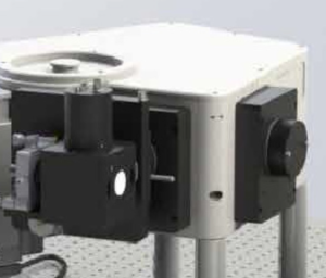
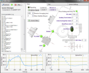
The company sourced Labsphere to design, build and deliver an automated spectroradiometer source of uniform spectral irradiance. The calibration system consisted of stable UV-VIS-NIR light sources, a monochromator, and filter wheel with ND filters and a blank for dark correction, monitor detector, Integrating sphere, apertures to control effective f/ #, a reference photodiode and signal conditioning electronics. The system was designed with real time traceable spectral irradiance monitoring at the sensor active area with user selectable fields of view.
| Objective | Benefits Achieved |
| Selecting appropriate sensors for OEM products | Reliable product quality and performance |
| Test multiple sensors with user defined illumination conditions with one system | Quantum efficiency characterization in intended application geometry |
| Optimize test time | With one universal system multiple tests are achieved for each device under test |